Course projects, from transistor-level circuit design to RTL and device modelling. Where a project was done in a team, the contribution of each member is listed.
Show:
10-bit Differential SAR ADC
EE 719 · Mixed-Signal VLSI Design · Spring 2026
Guide: Prof. Maryam Shojaei Baghini
Jatin Kumar (comparator controller, comparator and ADC integration, characterization) · Prajwal Nayak (capacitive DAC, DAC switches, SAR logic, final integration)
A 10-bit differential SAR ADC sampling at 200 MHz from a 1 V supply, with a 1 V differential full-scale range, designed in Cadence Virtuoso.
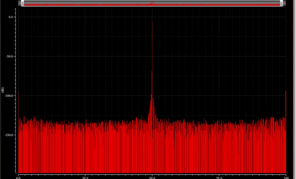
62.475 dB SNDR and 10.084-bit ENOB at 50 MHz input
Comparator controller: generates the comparison clock from the comparator's ready signal, with a 190 ps feedback inverter delay. The comparator resolves a 1 LSB input in about 238 ps, so at least 10 comparisons fit in the 4.5 ns hold phase of the 5 ns track-and-hold clock (10% track duty cycle).
Integrated the comparator, controller, capacitive DAC and SAR logic into the full converter and verified the SAR switching sequence against a hand-calculated output code.
Characterised the converter with a 4096-point coherent FFT. The ENOB from Cadence (10.084 bits) agrees with the value computed from SNDR to within 0.001 bit.
Measured INL and DNL with a differential ramp. A ramp that moves more than one LSB within a 5 ns conversion skips codes, so a slower 10240-cycle ramp was used to exercise every code.
FFT characterization.
Parameter
Value
Sampling frequency
200 MHz
Input frequency
50 MHz
FFT
4096 points, coherent, rectangular window
SNDR
62.475 dB
SFDR
62.51 dBc
ENOB
10.084 bits
FFT of the ADC output for a 50 MHz input, sampled at 200 MHz (4096 points).
Keywords: Mixed-signal, Cadence Virtuoso, MATLAB
InGaAs/AlInAsSb SACM Avalanche Photodiode for 1550 nm LiDAR
MM 618 · Optoelectronic Properties, Materials & Devices · Spring 2026
Guide: Prof. Tanushree H. Choudhury
Jatin Kumar · Sthiti Padhi
An electrical, optical and materials analysis of the separate-absorption-charge-multiplication (SACM) avalanche photodiode on InP, with an InGaAs absorber and an Al0.7In0.3As0.79Sb0.21 digital-alloy multiplier, for 1550 nm LiDAR detection.
Analysis of the device reported by B. Guo et al., APL Photonics8, 116112 (2023).
0.76 eV conduction-band offset · ~49% single-pass absorption at 1550 nm · 0.26% lattice mismatch to InP
Band alignment: band parameters and Anderson heterojunction offsets for every interface. The 0.76 eV conduction-band offset between InGaAs and AlInAsSb acts as an electron barrier at the blocking layer and is why the grading layers are needed.
Fermi levels: computed layer by layer with Boltzmann, Joyce–Dixon or exact Fermi–Dirac statistics, chosen from each layer's degeneracy. This corrected our mid-semester version, which used Boltzmann statistics throughout and was off by up to 0.27 eV in the most heavily doped layer.
Equilibrium: vacuum-level analysis gives a built-in potential of about 1.12 eV across the stack, with the multiplication layer fully depleted at equilibrium.
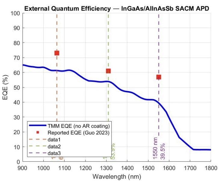
Optics: layer optical constants from Vegard's law, and a MATLAB transfer-matrix (TMM) model for the absorption and EQE. Single-pass absorption in the 1 µm InGaAs absorber is about 49.3% at 1550 nm. The simulated EQE lies below the reported values, which we attribute to bowing of the alloy refractive indices that Vegard's law does not capture.
Materials: lattice mismatch to InP of 0.26% from Vegard's law, and thermal strain after cooling from the 470 °C growth temperature of 4.9 × 10⁻⁴ in the absorber and 2.0 × 10⁻⁴ in the multiplier, both within the 5 × 10⁻⁴ elastic limit.
Noise: for the reported k = 0.02–0.04, McIntyre's model gives an excess noise factor of about 2.14 at a gain of 10, comparable to silicon. The reported maximum gain is about 17.
External quantum efficiency without an anti-reflection coating.
Wavelength
TMM model
Reported
1064 nm
62%
73%
1310 nm
53.9%
61%
1550 nm
39.5%
57%
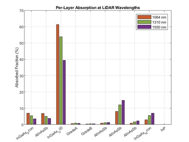
Simulated EQE (TMM, blue) against the values reported by Guo et al. (red markers).Fraction of light absorbed in each layer at 1064, 1310 and 1550 nm. Most is absorbed in the undoped InGaAs layer.
Keywords: Devices, MATLAB, TMM, Vegard's law
Matrix Multiplication: Loop Unrolling, Word Parallelism and Blocking
EE 789 · Algorithmic Design of Digital Systems · Spring 2026
Guide: Prof. Madhav Desai
Hardware design of a 64 × 64 int8 matrix multiplication in AHIR. The assignment first studies three optimisations separately; this part combines all three, cutting the run from 2,670,785 to 180,417 clock ticks. All 4096 outputs match the baseline.
14.8× fewer clock ticks than the naive baseline
Word parallelism: matrices are stored as 64-bit words that each pack eight int8 values (A row-major, B column-major), so a dot product reads 16 wide words instead of 128 byte-wide values.
A pipelined dot8 operator multiplies eight byte pairs in parallel and adds them in a three-level tree.
The remaining eight-iteration loop is fully unrolled, which removes its phi-merges, condition checks and branches.
The three optimisations target different bottlenecks (memory accesses, loop control and the serial accumulation), so their gains compound. Blocking alone did not help, since AHIR has no cache to exploit.
Clock ticks for the 64 × 64 multiplication.
Configuration
Ticks
Speedup
Naive baseline
2,670,785
1.00×
Loop unrolling only
1,749,185
1.53×
Word parallelism only
680,129
3.93×
Blocking only
2,691,265
0.99×
All three combined
180,417
14.8×
Keywords: Digital, AHIR
2×2 Packet Switches: Shared-, Input- and Output-Queued
EE 789 · Algorithmic Design of Digital Systems · Spring 2026
Guide: Prof. Madhav Desai
Three 2×2 packet switch architectures in VHDL-2008, built from one common packet FIFO and small arbiter state machines, and compared on queueing, fairness and head-of-line blocking.
Packets are sequences of 32-bit words. The header word holds an 8-bit destination, a 16-bit length and an 8-bit sequence ID, and packets are at most 64 words.
A parameterised FIFO with a combinational peek port lets an arbiter read a header without removing it. All three designs share this FIFO.
Every module is a small FSM (at most three states). Arbiters are round-robin, and a packet is served completely before the arbiter switches inputs.
Verified with three traffic scenarios (one active port, both ports to the same destination, both ports to different destinations), plus a test that shows head-of-line blocking in the input-queued design. Simulated with GHDL and inspected in GTKWave.
Comparison of the three architectures.
Shared-queue
Input-queued
Output-queued
FIFOs
1
2
4
Head-of-line blocking
No
Yes
No
Throughput under contention
Full
58.6% (theoretical limit)
Full
Hardware complexity
Low
Medium
High
Keywords: Digital, VHDL-2008, GHDL, GTKWave
Two-Stage OTA with Frequency Compensation
EE 618 · CMOS Analog VLSI Design · Autumn 2025
Guide: Prof. Rajesh Zele
A differential two-stage OTA, taken from schematic through full-custom layout and parasitic extraction.
63 dB gain · 118 MHz unity-gain frequency · 113 V/µs slew rate · 0.3 mW
Designed the amplifier in Cadence Virtuoso with RC and tracking compensation, reaching 63 dB gain, 118 MHz unity-gain frequency, 113 V/µs slew rate and 60–72° phase margin within a 0.3 mW power budget.
Drew a full-custom layout of 34.35 × 45 µm² with common-centroid matching and structured routing on the critical devices.
Cleared DRC and LVS, then ran Quantus parasitic extraction to validate the final layout.
Keywords: Analog, Cadence Virtuoso, Quantus
Noise Cancellation and Digital Filtering in Verilog
EE 671 · VLSI Design · Autumn 2024
Guide: Prof. Laxmeesha Somappa
Four noise-reduction filters in RTL, carried through synthesis, place-and-route and full-custom layout.
Implemented LMS, spectral subtraction, Wiener and median filters in Verilog, each with a testbench.
Synthesised with OpenLane, including floorplanning, placement and routing, and extracted timing and power metrics.
Drew full-custom layouts in Magic, ran DRC, LVS and antenna checks and fixed the violations to produce GDS-ready layouts, and weighed area, power and frequency trade-offs.